A deep dive into microcontroller architectures
Previously, we were discussing ATmega328P programming, diving into concepts like GPIO control, timers, and communication interfaces. However, before proceeding further into programming and advanced microcontroller operations, it is crucial to have a solid understanding of microcontroller architecture.
Microcontrollers are the backbone of modern embedded systems, powering a vast range of applications, from smart home devices to industrial automation. Understanding microcontroller architectures is essential for designing efficient and optimized embedded systems.
1. What is a Microcontroller?
A microcontroller (MCU) is a compact integrated circuit (IC) that contains a processor (CPU), memory (RAM, ROM, and Flash), and input/output peripherals on a single chip. Unlike general-purpose processors, microcontrollers are designed for specific control applications in embedded systems.
1.1 Role of Microcontrollers in Embedded Systems
Microcontrollers serve as the central control unit in a variety of embedded applications, including:
- Consumer Electronics – Smart TVs, home automation, wearables.
- Automotive Systems – Engine control units (ECUs), ABS systems.
- Industrial Automation – Programmable logic controllers (PLCs), robotics.
- Medical Devices – Pacemakers, glucose monitors.
1.2 Key Features of Microcontrollers
- Integrated CPU, Memory, and I/O Peripherals – Compact design for embedded applications.
- Power Efficiency – Low-power operation suitable for battery-powered systems.
- Real-Time Processing – Handles time-sensitive control tasks efficiently.
2. Microcontroller vs. Microprocessor
Microcontrollers and microprocessors serve different purposes, with distinct architectural differences.
| Feature | Microcontroller | Microprocessor |
|---|---|---|
| Primary Use | Embedded control applications | General-purpose computing |
| Components | CPU, RAM, ROM, I/O, timers | CPU only, requires external memory & peripherals |
| Power Consumption | Low | High |
| Processing Speed | Lower (few MHz to GHz) | Higher (GHz range) |
| Examples | ATmega328P, STM32, PIC16F877A | Intel Core i7, AMD Ryzen |
3. Microcontroller Architectures: Von Neumann vs. Harvard
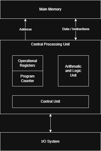
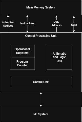
Microcontrollers follow two primary architectural designs: Von Neumann and Harvard. Understanding these architectures helps in selecting the right microcontroller for a given application.
| Feature | Von Neumann Architecture | Harvard Architecture |
|---|---|---|
| Memory Structure | Shared memory for program and data | Separate memory for program and data |
| Bus System | Single bus for instruction and data | Separate buses for instruction and data |
| Execution Speed | Slower due to memory bottleneck | Faster due to parallel access |
| Complexity | Simpler design | More complex hardware design |
| Power Consumption | Generally lower | Higher due to dual memory structure |
| Real-Time Processing | Less efficient for real-time applications | More efficient for real-time processing |
| Examples | Early x86 processors, some ARM Cortex-M | AVR (ATmega328P), ARM Cortex-M, DSP processors |


3.1 Von Neumann Architecture
The Von Neumann architecture, named after John von Neumann, features a single shared memory for both program instructions and data. This means that both instructions and data use the same bus, leading to a potential bottleneck in data transfer speed.
3.2 Harvard Architecture
The Harvard architecture features separate memory and buses for program instructions and data, allowing simultaneous instruction fetching and data access.
3.3 Modified Harvard Architecture
To balance flexibility and performance, modern microcontrollers often use a Modified Harvard Architecture, which allows selective data transfer between instruction and data memory.
Examples: ARM Cortex-M microcontrollers, which can access data memory in a Von Neumann-like manner while keeping separate program and instruction memory for efficiency.
4. Key Components of a Microcontroller CPU
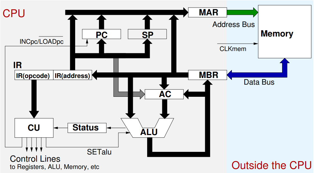
A microcontroller CPU consists of several interconnected units that work together to process instructions. I got this bog standerd architecture from one of the lectures of microcontroller architecture lectures from University of Oxford.

4.1 Arithmetic Logic Unit (ALU)
The ALU (Arithmetic Logic Unit) is responsible for executing arithmetic and logical operations. It performs operations such as:
- Arithmetic Operations: Addition, subtraction, multiplication, division.
- Logical Operations: AND, OR, XOR, NOT.
- Comparison Operations: Greater than, less than, equal to.
- Bitwise Operations: Bit shifting, bit masking, and rotation.
The ALU works in conjunction with registers and status flags to manage computational results. The Status Register (SR) holds flags such as:
- Zero Flag (Z) – Set if the result of an operation is zero.
- Carry Flag (C) – Set if an arithmetic operation results in a carry.
- Overflow Flag (V) – Set if an arithmetic operation exceeds bit limits.
- Negative Flag (N) – Set if the result of an operation is negative.
4.2 Control Unit (CU)
The Control Unit (CU) manages the flow of instructions within the CPU. It:
- Fetches instructions from memory.
- Decodes instructions to determine the operation.
- Executes the instruction by coordinating data flow between ALU, registers, and memory.
- Handles interrupts to manage real-time execution.
The CU operates using a sequence of control signals that regulate register transfers and ALU operations. It consists of:
- Instruction Decoder – Interprets opcode and determines operation.
- Timing and Control Logic – Synchronizes execution with the clock.
- Microprogram Unit – Generates control signals for complex instructions.
4.3 Registers
Registers are small, fast memory locations inside the CPU used for temporary data storage. Some important registers include:
- Program Counter (PC) – Stores the address of the next instruction to be executed.
- Instruction Register (IR) – Holds the current instruction being executed.
- Accumulator (AC) – A primary register for arithmetic/logical operations.
- Memory Address Register (MAR) – Holds the address of the memory location being accessed.
- Memory Buffer Register (MBR) – Temporarily stores data fetched from memory.
- Stack Pointer (SP) – Points to the top of the stack for function calls and interrupts.
- Status Register (SR) – Holds condition flags (Zero Flag, Carry Flag, Overflow Flag, etc.).
- General-Purpose Registers – Used for temporary storage of data.
5. The Fetch-Decode-Execute Cycle
The Fetch-Decode-Execute Cycle describes how a microcontroller processes instructions step by step.
5.1 Fetch Phase
- The Program Counter (PC) contains the memory address of the next instruction.
- The Memory Address Register (MAR) loads this address.
- The instruction is fetched from memory into the Memory Buffer Register (MBR).
- The instruction is moved from MBR to Instruction Register (IR).
5.2 Decode Phase
- The Control Unit (CU) deciphers the opcode (operation code) inside the Instruction Register (IR).
- The CU determines what action needs to be performed (arithmetic, logic, memory operation, or control flow change).
5.3 Execute Phase
- The ALU performs the required operation (e.g., addition, bitwise operation, data movement).
- The result is stored in the Accumulator (AC) or another register.
- Status flags in the Status Register (SR) are updated based on the outcome.
Once execution is complete, the Program Counter (PC) increments to fetch the next instruction, and the cycle repeats.
6. Example: Fetch-Decode-Execute Cycle in Action
Let’s take an example using simple assembly instructions for an 8-bit microcontroller.
Example Instruction Sequence:
LDA 0x10   ; Load value from memory address 0x10 into Accumulator
ADD 0x11   ; Add value from memory address 0x11 to Accumulator
STA 0x12   ; Store the result in memory address 0x12
Step-by-Step Execution:
- Fetch LDA 0x10
- PC → MAR → Memory fetches instruction
LDA 0x10. - MBR → IR, PC increments.
- PC → MAR → Memory fetches instruction
- Decode LDA
- CU recognizes opcode
LDA, identifies operand0x10.
- CU recognizes opcode
- Execute LDA
- Memory at
0x10→ AC.
- Memory at
- Fetch ADD 0x11
- PC → MAR → Memory fetches instruction
ADD 0x11. - MBR → IR, PC increments.
- PC → MAR → Memory fetches instruction
- Decode ADD
- CU recognizes
ADD, identifies operand0x11.
- CU recognizes
- Execute ADD
- AC + Memory at
0x11→ AC (ALU operation).
- AC + Memory at
- Fetch STA 0x12
- PC → MAR → Memory fetches instruction
STA 0x12. - MBR → IR, PC increments.
- PC → MAR → Memory fetches instruction
- Decode STA
- CU recognizes
STA, identifies operand0x12.
- CU recognizes
- Execute STA
- AC → Memory at
0x12.
- AC → Memory at
After execution, the result is stored in memory at 0x12, and the CPU continues processing the next instruction.
In this post, we explored microcontroller architectures, covering Von Neumann and Harvard designs, followed by a deep dive into the CPU’s internal components such as the ALU, Control Unit, and Registers. We then examined the Fetch-Decode-Execute Cycle step-by-step, using a practical example to illustrate how instructions are processed within a microcontroller.
Understanding these fundamental concepts provides a strong foundation for designing efficient embedded systems and optimizing microcontroller-based applications. As we move forward, we will delve into microcontroller memory systems, including RAM, ROM, EEPROM, and memory addressing techniques, to understand how microcontrollers handle data storage and retrieval.
Stay tuned for the next post in this series, where we will explore microcontroller memory systems in depth!
Enjoy Reading This Article?
Here are some more articles you might like to read next: